- 您现在的位置:买卖IC网 > Sheet目录17360 > REF198GRUZ (Analog Devices Inc)IC VREF SRS PREC 4.096V 8-TSSOP
Data Sheet
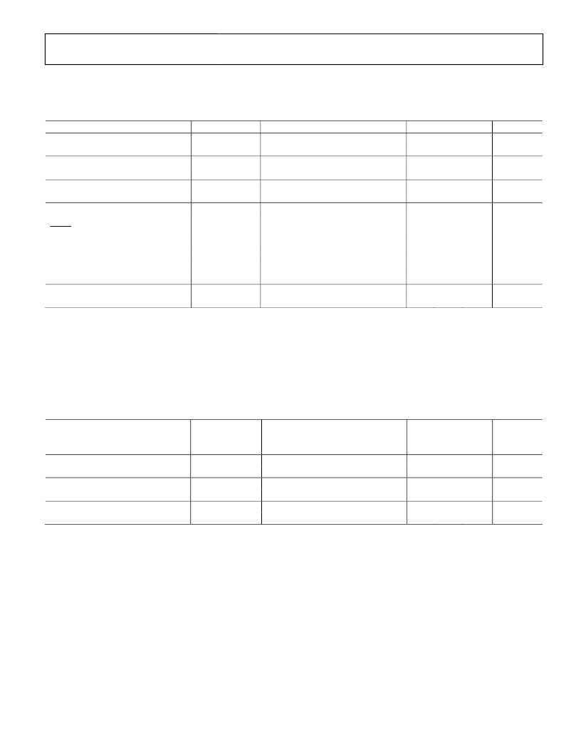
ELECTRICAL CHARACTERISTICS—REF196 @ ? 40°C ≤ T A ≤ +85°C
@ V S = 3.5 V, T A = –40°C ≤ T A ≤ +85°C, unless otherwise noted.
Table 18.
REF19x Series
Parameter
Symbol
Condition
Min
Typ
Max
Unit
TEMPERATURE COEFFICIENT 1, 2
TCV O /°C
G Grade 3
I OUT = 0 mA
10
25
ppm/°C
LINE REGULATION 4
ΔV O /ΔV IN
G Grade
3.5 V ≤ V S ≤ 15 V, I OUT = 0 mA
10
20
ppm/V
LOAD REGULATION 4
ΔV O /ΔV LOAD
G Grade
V S = 5.0 V, 0 mA ≤ I OUT ≤ 25 mA
10
20
ppm/mA
DROPOUT VOLTAGE
V S ? V O
V S = 4.1 V, I LOAD = 10 mA
V S = 4.3 V, I LOAD = 25 mA
0.80
1.00
V
V
SLEEP PIN
Logic High Input Voltage
Logic High Input Current
Logic Low Input Voltage
Logic Low Input Current
SUPPLY CURRENT
Sleep Mode
V H
I H
V L
I L
No load
No load
2.4
?8
0.8
?8
45
15
V
μA
V
μA
μA
μA
1
2
3
4
For proper operation, a 1 μF capacitor is required between the output pin and the GND pin of the device.
TCV O is defined as the ratio of output change with temperature variation to the specified temperature range expressed in ppm/°C.
TCV O = ( V MAX ? V MIN )/ V 0 ( T MAX ? T MIN )
Guaranteed by characterization.
Line and load regulation specifications include the effect of self-heating.
ELECTRICAL CHARACTERISTICS—REF196 @ ? 40°C ≤ T A ≤ +125°C
@ V S = 3.50 V, ?40°C ≤ T A ≤ +125°C, unless otherwise noted.
Table 19.
Parameter
Symbol
Condition
Min
Typ
Max
Unit
TCV O /°C
G Grade 3
LINE REGULATION 4
G Grade
LOAD REGULATION 4
G Grade
ΔV O /ΔV IN
ΔV O /ΔV LOAD
I OUT = 0 mA
3.50 V ≤ V S ≤ 15 V, I OUT = 0 mA
V S = 5.0 V, 0 mA ≤ I OUT ≤ 20 mA
10
20
20
ppm/°C
ppm/V
ppm/mA
DROPOUT VOLTAGE
V S ? V O
V S = 4.1 V, I LOAD = 10 mA
V S = 4.4 V, I LOAD = 20 mA
0.80
1.10
V
V
1
2
3
4
For proper operation, a 1 μF capacitor is required between the output pin and the GND pin of the device.
TCV O is defined as the ratio of output change with temperature variation to the specified temperature range expressed in ppm/°C.
TCV O = ( V MAX ? V MIN )/ V O ( T MAX ? T MIN )
Guaranteed by characterization.
Line and load regulation specifications include the effect of self-heating.
Rev. L | Page 13 of 28
发布紧急采购,3分钟左右您将得到回复。
相关PDF资料
RB-153.3S/H
CONV DC/DC 1W 15VIN 3.3VOUT
F971V475MCC
CAP TANT 4.7UF 35V 20% 2312
IRDC3710-DF
BOARD EVAL SYNC BUCK CONTROLLER
F971E106MCC
CAP TANT 10UF 25V 20% 2312
RB-1524S/H
CONV DC/DC 1W 15VIN 24VOUT
MIC2545A-2BM TR
IC SW CURR LIMIT HI SIDE 8-SOP
ZXRE125DN8TA
IC VREF SHUNT PREC 1.22V 8-SO
RB-1515S/H
CONV DC/DC 1W 15VIN 15VOUT
相关代理商/技术参数
REF198GRUZ
制造商:Analog Devices 功能描述:VOLTAGE REFERENCE, BOOST, 4.096V, TSSOP-
REF198GRUZ-REEL7
功能描述:IC VREF SRS PREC 4.096V 8-TSSOP RoHS:是 类别:集成电路 (IC) >> PMIC - 电压基准 系列:REF19 标准包装:2,000 系列:- 基准类型:旁路,可调节,精度 输出电压:1.24 V ~ 16 V 容差:±0.5% 温度系数:- 输入电压:1.24 V ~ 16 V 通道数:1 电流 - 阴极:100µA 电流 - 静态:- 电流 - 输出:20mA 工作温度:-40°C ~ 85°C 安装类型:通孔 封装/外壳:TO-226-3、TO-92-3(TO-226AA)成形引线 供应商设备封装:TO-92-3 包装:带卷 (TR)
REF198GS
功能描述:IC VREF SERIES PREC 4.096V 8SOIC RoHS:否 类别:集成电路 (IC) >> PMIC - 电压基准 系列:REF19 标准包装:3,000 系列:- 基准类型:旁路,精度 输出电压:5V 容差:±0.5% 温度系数:100ppm/°C 输入电压:- 通道数:1 电流 - 阴极:80µA 电流 - 静态:- 电流 - 输出:15mA 工作温度:-40°C ~ 85°C 安装类型:表面贴装 封装/外壳:TO-236-3,SC-59,SOT-23-3 供应商设备封装:SOT-23-3 包装:带卷 (TR) 其它名称:LM4040CIM3-5.0MLTRLM4040CIM3-5.0MLTR-ND
REF198GS-REEL
功能描述:IC VREF SERIES PREC 4.096V 8SOIC RoHS:否 类别:集成电路 (IC) >> PMIC - 电压基准 系列:REF19 标准包装:3,000 系列:- 基准类型:旁路,精度 输出电压:5V 容差:±0.5% 温度系数:100ppm/°C 输入电压:- 通道数:1 电流 - 阴极:80µA 电流 - 静态:- 电流 - 输出:15mA 工作温度:-40°C ~ 85°C 安装类型:表面贴装 封装/外壳:TO-236-3,SC-59,SOT-23-3 供应商设备封装:SOT-23-3 包装:带卷 (TR) 其它名称:LM4040CIM3-5.0MLTRLM4040CIM3-5.0MLTR-ND
REF198GSZ
功能描述:IC VREF SERIES PREC 4.096V 8SOIC RoHS:是 类别:集成电路 (IC) >> PMIC - 电压基准 系列:REF19 标准包装:3,000 系列:- 基准类型:旁路,精度 输出电压:3V 容差:±0.5% 温度系数:100ppm/°C 输入电压:- 通道数:1 电流 - 阴极:82µA 电流 - 静态:- 电流 - 输出:15mA 工作温度:-40°C ~ 85°C 安装类型:表面贴装 封装/外壳:6-TSSOP(5 引线),SC-88A,SOT-353 供应商设备封装:SC-70-5 包装:带卷 (TR) 其它名称:296-20888-2
REF198GSZ
制造商:Analog Devices 功能描述:Voltage Reference
REF198GSZ-REEL
功能描述:IC VREF SERIES PREC 4.096V 8SOIC RoHS:是 类别:集成电路 (IC) >> PMIC - 电压基准 系列:REF19 产品培训模块:Voltage Reference Basics 标准包装:100 系列:- 基准类型:旁路,精度 输出电压:4.096V 容差:±0.075% 温度系数:50ppm/°C 输入电压:- 通道数:1 电流 - 阴极:1µA 电流 - 静态:- 电流 - 输出:10mA 工作温度:0°C ~ 70°C 安装类型:表面贴装 封装/外壳:8-SOIC(0.154",3.90mm 宽) 供应商设备封装:8-SOIC 包装:管件
REF19X
制造商:AD 制造商全称:Analog Devices 功能描述:Precision Micropower, Low Dropout Voltage References
